If you’ve worked in electronics design for any length of time, odds are you’ve sat at a lab bench staring at a circuit that won’t perform quite right, wondering why. Half the time the culprit isn’t a flaw in your layout or a wrong value resistor—it’s the humble transistor. For all the incredible things these tiny components do, they come with built-in limitations that have stumped designers for decades. As someone who’s spent 12 years selling transistors for a component supplier, I’ve sat through hundreds of these conversations: engineers complaining about gain rolloff at high frequencies, thermal drift that throws off sensor circuits, or hard switching that causes unwanted noise. The good news? Most of these limitations aren’t permanent. They just require a mix of smart design tweaks, component selection, and a deep understanding of how transistors actually behave in real-world conditions. Transistor
Let’s start with the most common limitation of all: frequency response. Bipolar junction transistors (BJTs) and even modern MOSFETs both suffer from gain rolloff as signal frequency climbs. This happens because of internal capacitances—things like the base-emitter capacitance in a BJT or the gate-drain capacitance in a MOSFET—that start shunting signal current to ground once frequency hits the transistor’s cutoff frequency. A designer I worked with last year was building a 2.4 GHz wireless sensor node and couldn’t get his amplifier to hit the required gain. He was using a generic NPN BJT we stock for low-frequency switching, and when I checked the datasheet, its transition frequency (fT) was only 300 MHz. No wonder it fell apart at 2.4 GHz. The fix here is simpler than you might think: select a transistor rated for the frequency range you’re working in. For high-frequency applications like RF or 5G frontends, that means choosing transistors designed specifically for that space—like LDMOS FETs or gallium arsenide (GaAs) HBTs, which have fT values in the tens of GHz. But frequency isn’t just about the transistor itself. A small design tweak can stretch your current part’s usable range too: adding a small inductor in series with the collector or drain creates a resonant tank that cancels out those parasitic capacitances at your target frequency. That trick helped another customer of ours get an extra 500 MHz of usable gain from a part they already had on hand, saving them from a last-minute component respin.
Next up: thermal performance. Transistors generate heat when current flows through them, and excess heat changes their electrical characteristics, reduces lifespan, and can even cause catastrophic failure. The most familiar example is thermal runaway in power BJTs, where increasing temperature makes the transistor conduct more current, which makes it hotter, and so on in a vicious cycle. I remember a customer designing a 100 watt audio amplifier that kept blowing output transistors mid-burn-in. They’d mounted the TO-220 packaged transistors on a thin fiberglass PCB, with no heatsink, and wondered why they were failing. The fix here is twofold. First, pay close attention to the transistor’s thermal resistance rating (θJC, the junction-to-case thermal resistance, and θJA, the junction-to-ambient resistance). A TO-220 package has a much lower θJC than a surface-mount chip for power applications, because it can transfer heat to a heatsink directly. Second, use a thermal interface material (TIM) between the transistor’s case and the heatsink—even a thin layer of thermal grease or a thermal pad reduces air gaps that act as insulators. For high-power designs, you can also parallel transistors to split the current load, which cuts the heat generated per part. Just make sure you match the transistors as closely as possible for VBE (for BJTs) or gate threshold (for MOSFETs) to avoid current hogging, where one part carries most of the load and overheats.
Then there’s switching speed, a critical limitation for power electronics like motor drivers or switching power supplies. Slow switching transistors waste energy as heat during the transition between on and off states, and they can cause voltage spikes that damage other components. MOSFETs are particularly prone to this because their gate capacitance needs to charge and discharge before the transistor turns on or off. I had a customer building a brushless DC motor controller that had 10% higher power draw than their target, traced right back to the MOSFET switching losses. The solution here starts with gate resistance. Most MOSFET datasheets list a recommended gate resistor value that balances speed and noise; too low and you get voltage spikes, too high and switching is slow. We often suggest trying a few different gate resistors in 10Ω increments to find the sweet spot for your design. Another trick is using a gate driver IC, which can supply the high current needed to charge the MOSFET’s gate capacitance much faster than a microcontroller I/O pin can. For even faster switching, consider silicon carbide (SiC) MOSFETs or gallium nitride (GaN) transistors. These wide-bandgap (WBG) parts have much lower switching losses than silicon MOSFETs, and they’ve become far more affordable over the last five years—we’ve seen demand for GaN parts jump 40% since 2021, exactly because designers are switching from silicon to solve switching speed issues.
One limitation that’s less talked about but equally frustrating is linearity, especially in analog applications like audio amplifiers or precision signal processing. Transistors don’t amplify signals perfectly; at high signal levels, they enter saturation (for BJTs) or the triode region (for MOSFETs), distorting the input signal. I once worked with an audio equipment maker that was getting negative reviews for “muddy” bass in their new amp, and the issue was that they were using a single transistor in the amplification stage, which created harmonic distortion. The fix here isn’t always swapping the part—though choosing a linear BJT or a MOSFET with high transconductance can help—but rather adding circuit topology. Push-pull configurations, where two transistors (one for the positive half of the signal, one for the negative) work together, eliminate crossover distortion common in single-ended designs. Or, for precision applications, use an op-amp with discrete transistor output stages, but even a well-designed single BJT with a resistor in the emitter can improve linearity by stabilizing the operating point. It’s also worth noting that not all transistors are created equal for linearity: parts labeled as “audio-grade” undergo tighter manufacturing tolerances to ensure consistent gain across their operating range, so they’re worth the slight premium for analog designs.
Another persistent limitation is reliability in harsh environments. Transistors exposed to high humidity, temperature extremes, vibration, or corrosive gases can fail prematurely, often due to package degradation or bond wire failure. We supply a lot of transistors to aerospace, industrial automation, and automotive clients, and this is a top concern for them. The first step here is selecting a transistor package rated for environmental stress. For example, a plastic DIP package isn’t suitable for -40°C to 125°C industrial use, but an hermetically sealed ceramic package is. For automotive applications, look for AEC-Q100 qualified parts, which undergo extensive testing for temperature cycling, vibration, and moisture resistance. We recently helped an agricultural equipment manufacturer switch from a standard surface-mount MOSFET to an AEC-Q100 qualified one, and they cut field failure rates by 92% in their harvester motor controllers, which are exposed to dust, rain, and extreme temperature swings year-round. Additionally, adding conformal coating to your PCB and transistors can block moisture and corrosive gases, a cheap add-on that makes a huge difference for outdoor or industrial designs.
Wait, let’s touch on something that’s been top of mind for a lot of our customers lately: the tradeoff between on-resistance (Rdson) and gate charge in MOSFETs. It’s a classic design dilemma: a MOSFET with low Rdson is more efficient when on, but it has higher gate charge, meaning it takes longer to switch, leading to higher switching losses. The opposite is also true. This is a real limitation for power supply designers, who have to balance efficiency at idle vs. full load. A telecom customer came to us last year trying to optimize a 48V power supply for both light-load efficiency and peak load performance, and they were stuck because every MOSFET we suggested traded off one for the other. The solution here was to use a synchronous rectifier design with different MOSFETs for light and full load, or to choose a super-junction MOSFET, which manages this tradeoff much better than traditional planar MOSFETs. Super-junction parts use a unique internal structure to reduce Rdson without increasing gate charge, and they’ve become the go-to for high-efficiency power electronics over the last decade. For our customer, switching to a super-junction MOSFET let them hit both their light-load and peak efficiency targets without needing extra components, saving them board space and cost.
I think it’s important to frame all this not as “transistors are flawed,” but as “transistors are components with specific operating limits, and working within (or around) those limits is what good design is all about.” Over my 12 years in this industry, I’ve seen too many designers write off a transistor too quickly, or try to force a part into an application it was never meant for. When that happens, the first call we get is usually to help troubleshoot, and 9 times out of 10, the fix is not a replacement with a more expensive part—though sometimes that’s needed—but a small adjustment in design, or a more careful selection of the right part for the job.
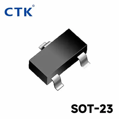
For example, I once had a startup that was building a portable medical device and trying to use a tiny SOT-23 packaged MOSFET for the power switching. They were getting overheating issues because the small package couldn’t dissipate heat enough for their 5W load. Instead of moving to a larger package that would take up too much space on their small PCB, we suggested a DFN package with exposed pad, which has a much lower thermal resistance than a standard SOT-23, and it’s small enough to fit their board design. That solved their problem perfectly, no respin needed.
The key takeaway here is that overcoming transistor limitations is a mix of science and practical experience. It means understanding your application’s specific needs—frequency, power, environment, size—and matching that to the right transistor’s datasheet specs, then tweaking the circuit to work with the part, not against it. That’s where we come in. As a transistor supplier, we don’t just sell parts—we work with designers to walk through these exact challenges. Whether you’re troubleshooting a frequency rolloff issue, dealing with thermal runaway, stuck on the Rdson/gate charge tradeoff, or looking for a more reliable part for a harsh environment, we can help you navigate the options and find the solution that fits your design. We’ve supported thousands of engineers across industries—automotive, industrial, aerospace, consumer electronics, medical—so we’ve likely seen a similar challenge before. If you’re hitting a wall with your transistor design, we encourage you to reach out to discuss your requirements and explore the best solutions for your project.
Transistors References:
- Neamen, D. A. (2021). Semiconductor Physics and Devices: Basic Principles. McGraw-Hill.
- Sedra, A. S., & Smith, K. C. (2020). Microelectronic Circuits (8th ed.). Oxford University Press.
- Baliga, B. J. (2008). Fundamentals of Power Semiconductor Devices. Springer.
- Hormilton, D. (2022). “GaN and SiC MOSFETs: Market Trends and Performance Improvements.” IEEE Industrial Electronics Magazine.
Tongke Electronic Co., Ltd
Tongke Electronic Co., Ltd. is one of the most experienced transistor manufacturers and suppliers in China, featured by quality products and low price. Please rest assured to wholesale advanced transistor made in China here from our factory. Contact us for pricelist.
Address: No.3,Chayuan Rd, Street 3, AilingKan, Dalingshan, Dongguan, Guangdong, China.
E-mail: jack@ctk-elec.com
WebSite: https://www.ctkchip.com/
